- 您現(xiàn)在的位置:買(mǎi)賣(mài)IC網(wǎng) > PDF目錄382287 > MAX9022ASA (MAXIM INTEGRATED PRODUCTS INC) Octal Buffers/Drivers With 3-State Outputs 20-CFP -55 to 125 PDF資料下載
參數(shù)資料
| 型號(hào): | MAX9022ASA |
| 廠商: | MAXIM INTEGRATED PRODUCTS INC |
| 元件分類(lèi): | 運(yùn)動(dòng)控制電子 |
| 英文描述: | Octal Buffers/Drivers With 3-State Outputs 20-CFP -55 to 125 |
| 中文描述: | DUAL COMPARATOR, 8000 uV OFFSET-MAX, PDSO8 |
| 封裝: | SO-8 |
| 文件頁(yè)數(shù): | 2/8頁(yè) |
| 文件大小: | 353K |
| 代理商: | MAX9022ASA |
M
Micropower, Ultra-Small, Single/Dual/Quad,
Single-Supply Comparators
2
_______________________________________________________________________________________
ABSOLUTE MAXIMUM RATINGS
Supply Voltage (V
DD
to V
SS
)....................................-0.3V to +6V
Voltage Inputs (IN+, IN- to V
SS
).................-0.3V to (V
DD
+ 0.3V)
Differential Input Voltage (IN+ to IN-)....................................6.6V
Output Short-Circuit Duration..................2s to Either V
DD
or V
SS
Current into Any Pin............................................................20mA
Continuous Power Dissipation (T
A
= +70
°
C)
5-Pin SC70 (derate 3.1mW/
°
C above +70
°
C)...............247mW
5-Pin SOT23 (derate 7.1mW/
°
C above +70
°
C).............571mW
8-Pin SOT23 (derate 9.1mW/
°
C above +70
°
C).............727mW
Stresses beyond those listed under “Absolute Maximum Ratings” may cause permanent damage to the device. These are stress ratings only, and functional
operation of the device at these or any other conditions beyond those indicated in the operational sections of the specifications is not implied. Exposure to
absolute maximum rating conditions for extended periods may affect device reliability.
8-Pin μMAX (derate 4.5mW/
°
C above +70
°
C)..............362mW
8-Pin SO (derate 5.88mW/
°
C above +70
°
C).................471mW
14-Pin TSSOP (derate 9.1mW/
°
C above +70
°
C) ..........727mW
14-Pin SO (derate 8.3mW/
°
C above +70.......................667mW
Operating Temperature Range
Automotive Application...................................-40
°
C to +125
°
C
Junction Temperature......................................................+150
°
C
Storage Temperature Range.............................-65
°
C to +150
°
C
Lead Temperature (soldering, 10s).................................+300
°
C
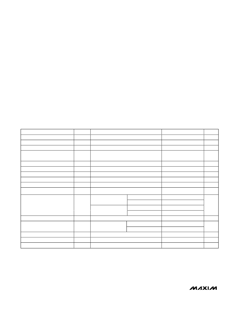
PARAMETER
SYMBOL
V
DD
I
DD
V
OS
CONDITIONS
MIN
2.5
TYP
MAX
5.5
5
±
8
UNITS
V
μA
mV
Operating Voltage Range
S up p y C ur ent P er C om p ar ator
Input Offset Voltage
Guaranteed by PSRR test
2.8
±
1
(Note 2)
Input Offset Voltage
Temperature Coefficient
TCV
OS
±
1
μV/
°
C
Hysteresis
Input Bias Current
Input Offset Current
Common-Mode Voltage Range
C om m on- M od e Rej ecti on Rati o
(Note 3)
4
3
±
2
mV
nA
nA
V
d B
I
BIAS
I
OS
V
CM
CMRR
80
±
60
Guaranteed by CMRR test
V
S S
≤
V
C M
≤
( V
D D
- 1.1V V
D D
= 5.5V
V
SS
70
V
DD
- 1.1
100
Power-Supply Rejection Ratio
PSRR
V
DD
= 2.5V to 5.5V
60
80
dB
I
SOURCE
= 10μA
I
SOURCE
= 4mA
I
SINK
= 10μA
I
SINK
= 4mA
2
V
OH
= V
DD
- V
OUT,
(V
IN+
- V
IN-
)
≥
20mV
160
2
180
50
8
3
20
150
150
400
Output-Voltage Swing
V
OL
, V
OH
V
OL
= V
OUT
- V
SS,
(V
IN-
- V
IN+
)
≥
20mV
400
mV
Output Short-Circuit Current
I
SC
m A
V
OD
= 10mV
V
OD
= 100mV
Propagation Delay
t
pd+
, t
pd
-
R
L
= 10k
,
C
L
= 15pF (Note 4)
R
L
= 10k
, C
L
= 15pF (Note 5)
R
L
= 10k
, C
L
= 15pF
No sustained oscillations
μs
Rise and Fall Time
Power-On Time
Maximum Capacitive Load
t
R
, t
F
ns
ns
pF
C
L
Note 1:
All devices are production tested at 25
°
C. All temperature limits are guaranteed by design.
Note 2:
Comparator Input Offset is defined as the center of the hysteresis zone.
Note 3:
Hysteresis is defined as the difference of the trip points required to change comparator output states.
Note 4:
V
OD
is the overdrive voltage beyond the offset and hysteresis-determined trip points.
Note 5:
Rise and fall times are measured between 10% and 90% at OUT.
ELECTRICAL CHARACTERISTICS
(V
DD
= 5V, V
SS
= 0, V
CM
= 0, T
A
= -40
°
C to +125
°
C, unless otherwise noted. Typical values are at T
A
= +25
°
C.) (Note 1)
相關(guān)PDF資料 |
PDF描述 |
|---|---|
| MAX9024 | Octal Bus Transceivers With 3-State Outputs 20-LCCC -55 to 125 |
| MAX9024AUD | DIODE ZENER 12V 200MW MINI 3P |
| MAX9021 | Octal Buffers/Drivers With 3-State Outputs 20-LCCC -55 to 125 |
| MAX9022 | Octal Buffers/Drivers With 3-State Outputs 20-CDIP -55 to 125 |
| MAX9021AUK-T | Micropower, Ultra-Small, Single/Dual/Quad, Single-Supply Comparators |
相關(guān)代理商/技術(shù)參數(shù) |
參數(shù)描述 |
|---|---|
| MAX9022ASA+ | 功能描述:校驗(yàn)器 IC Dual uPower Comparator RoHS:否 制造商:STMicroelectronics 產(chǎn)品: 比較器類(lèi)型: 通道數(shù)量: 輸出類(lèi)型:Push-Pull 電源電壓-最大:5.5 V 電源電壓-最小:1.1 V 補(bǔ)償電壓(最大值):6 mV 電源電流(最大值):1350 nA 響應(yīng)時(shí)間: 最大工作溫度:+ 125 C 安裝風(fēng)格:SMD/SMT 封裝 / 箱體:SC-70-5 封裝:Reel |
| MAX9022ASA+T | 功能描述:校驗(yàn)器 IC Dual uPower Comparator RoHS:否 制造商:STMicroelectronics 產(chǎn)品: 比較器類(lèi)型: 通道數(shù)量: 輸出類(lèi)型:Push-Pull 電源電壓-最大:5.5 V 電源電壓-最小:1.1 V 補(bǔ)償電壓(最大值):6 mV 電源電流(最大值):1350 nA 響應(yīng)時(shí)間: 最大工作溫度:+ 125 C 安裝風(fēng)格:SMD/SMT 封裝 / 箱體:SC-70-5 封裝:Reel |
| MAX9022ASA-T | 功能描述:校驗(yàn)器 IC Dual uPower Comparator RoHS:否 制造商:STMicroelectronics 產(chǎn)品: 比較器類(lèi)型: 通道數(shù)量: 輸出類(lèi)型:Push-Pull 電源電壓-最大:5.5 V 電源電壓-最小:1.1 V 補(bǔ)償電壓(最大值):6 mV 電源電流(最大值):1350 nA 響應(yīng)時(shí)間: 最大工作溫度:+ 125 C 安裝風(fēng)格:SMD/SMT 封裝 / 箱體:SC-70-5 封裝:Reel |
| MAX9022AUA | 功能描述:校驗(yàn)器 IC Dual uPower Comparator RoHS:否 制造商:STMicroelectronics 產(chǎn)品: 比較器類(lèi)型: 通道數(shù)量: 輸出類(lèi)型:Push-Pull 電源電壓-最大:5.5 V 電源電壓-最小:1.1 V 補(bǔ)償電壓(最大值):6 mV 電源電流(最大值):1350 nA 響應(yīng)時(shí)間: 最大工作溫度:+ 125 C 安裝風(fēng)格:SMD/SMT 封裝 / 箱體:SC-70-5 封裝:Reel |
| MAX9022AUA+ | 功能描述:校驗(yàn)器 IC Dual uPower Comparator RoHS:否 制造商:STMicroelectronics 產(chǎn)品: 比較器類(lèi)型: 通道數(shù)量: 輸出類(lèi)型:Push-Pull 電源電壓-最大:5.5 V 電源電壓-最小:1.1 V 補(bǔ)償電壓(最大值):6 mV 電源電流(最大值):1350 nA 響應(yīng)時(shí)間: 最大工作溫度:+ 125 C 安裝風(fēng)格:SMD/SMT 封裝 / 箱體:SC-70-5 封裝:Reel |
發(fā)布緊急采購(gòu),3分鐘左右您將得到回復(fù)。